
扫描电镜结合能谱仪揭示LCD的失效 发布时间:2021-07-01
Find out why LCDs fail
The combination of SEM and EDX techniques and reveal why inactive lines in LCD screens can appear.
Mark Woolley and Jae Choi, Avaya -- Test & Measurement World, 2/29/2012 2:17:45 PM
The TFT (thin-film transistor) LCD devices found in so many products are manufactured using semiconductor processes that deposit materials on a glass substrate. Because of their small size, TFT LCDs are subject to many of the same failure modes as semiconductor ICs. Two methods of inspecting TFT displays, those using SEMs (Scanning Electron Microscopes) and EDX (Energy Dispersive X-ray Spectroscopy) typically analyze surfaces only. The penetration depths of their electron beams are limited.
When the column voltage is high enough, however, penetration of electrons can reach 1?m into the materials. Often, that's deep enough for you to determine the composition of an underlayer of materials. Used in conjunction, SEM and EDX technologies can help you determine the cause of a failure.
An SEM produces black-and-white images using electrons generated in a reaction with the electrons in the source beam. The images show basic topology, but they contain little information concerning the elements present. The simultaneous use of an EDX detector can indicate what elements are present in the sample as well. Combining these two technologies can be useful in determining the cause of a failure.
Color TFT LCD displays are manufactured using layered of metal that form conductors on the glass. The conductors carry voltages and currents to the source and gate of each TFT in the viewing area. To reduce the number of conductors, the TFTs sources are connected in vertical columns while the gates are connected in horizontal rows. Individual pixels are turned on through scanning techniques.
The gate conductors are routed along the bottom of the glass panel, toward the left and right edges, and then along the edges to the appropriate row of transistors in the viewing area. The source conductors for the transistors are routed nearer the center of the glass panel and connect the sources in vertical columns. That makes the TFT's gate conductors longer than the source conductors and the gates are located more peripherally on the display glass panel. Because of this arrangement, the gate conductors are more susceptible to damage than the source conductors.
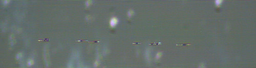
Visual inspection detected defects in the conductors that related to the inactive rows of pixels. Figure 1 shows an area of conductors that carry signals to the TFT gates. The image shows multiple defective conductors. Although multiple conductors have damage, each damage location affects only one conductor. A sharp instrument could damage multiple conductors, but the damage would be in a continuous line, not scattered as seen in this image.
Each conductor in Figure 1 is 5?m wide. The damage was very localized and wasn't caused by a large tool such as tweezers, because tweezers are much larger.

SEM analysis
To produce the image of the damage, we used an SEM with a 20-keV beam energy. The 20-keV beam causes electrons to penetrate approximately 1?m below the surface. Two areas were selected for further analysis. The area shown in Figure 2 has obvious damage to the passivation layer that covers the conductors. (SEM image constructed from secondary electrons.)
Figure 3 shows an anomalous region of a conductor that's darker than it neighbors. We selected as a site because of the anomaly. The SEM found no damage to the passivation layer over the conductor. Only the conductor had been affected.
EDX mapping
We then applied EDX mapping to the area shown in Figure 2. The main elements detected were silicon, aluminum, and molybdenum. We made maps for these three elements at a lower magnification. Figure 4 shows the image captured and the elemental maps.

There are several pieces of information that can be gleaned from this image.

The entire panel is manufactured on glass. The elements present in the glass are silicon, calcium, oxygen and sodium. We excluded oxygen from the map because it is also in silicon dioxide. In the mapping of this area, no sodium or calcium was noted. This suggests that the glass was coated with a passivation layer (SiO2) before starting to build the metal conductors.
The aluminum and molybdenum are mapped as white dots on the display. The brighter the area, the greater abundance of x-rays specific to these elements.
The aluminum map shows a long stretch of conductor that is missing aluminum. This begins at the damaged site and extends to the right in the map.
Molybdenum is less bright than aluminum because the characteristic x-rays aren't generated as easily under these conditions. There is, however, a definite area that's nearly devoid of molybdenum. This missing molybdenum is at the damage site.
A silicon map shows that the amount of silicon detected is greater in between the conductors. The metal in the conductors dramatically reduces the penetration of the electrons to the silicon beneath them. Only the silicon in the passivation layer on top of the conductors is imaged. Between the conductors, the electrons can penetrate through the top passivation into the passivation layer deposited on the glass.
A bright area in the silicon map is co-located with the missing aluminum. This indicates that the aluminum metallization is missing in this area allowing the electrons to penetrate deeply into the bottom passivation layer.
We then applied EDX mapping to the area shown in Figure 3. The results appear in Figure 5. Using the same logic as above, we made the following conclusions:
No damage to the top layer of passivation is noted in the damaged area.
There is a relatively long section of missing aluminum.
A much smaller section of the conductor lacks molybdenum as well.
The molybdenum along does not prevent electron penetration so the layer is thin.

Passivation damage can occur for a variety of reasons, including particulate contamination during the deposition, imaging, and etch processes, or during the subsequent manufacturing operation necessary to produce a display. It may even occur as a result of thermal damage. SEM alone shows that much. But, SEM alone didn't show us what was occurring in Figure 3 where there was an open circuit but no damage to the passivation.
These failures were probably built into the product during the deposition of the metallization on the glass panels. The creation of conductors such as this incorporates several cycles of metal deposition, photoresist application, imaging, and development and wet chemical etching. At any of these steps, problems with the adhesion of the photoresist or etching of the metal beneath the resist would create these apparent gaps in the conductor.
Mark Woolley is a failure analyst with over 30 years experience working in the semiconductor and electronics industries. He is the lead analyst in the Product Technology and Reliability Laboratory (PTRL Laboratory). He has three patents and the author of articles spanning the electronics and failure analysis areas.
Jae Choi, PhD is the manager of the laboratory at Avaya, Inc. He has authored several papers on the polymerization and manufacturing of plastics.
- 上一篇: 液晶ITO薄膜分析
- 下一篇: 扫描电镜应用之:锂离子电池材料